- 您现在的位置:买卖IC网 > Sheet目录1997 > ICS841602AGILF (IDT, Integrated Device Technology Inc)IC CLOCK GENERATOR 28-TSSOP
IDT / ICS HCSL CLOCK GENERATOR
9
ICS841602AGI REV. A JULY 10, 2008
ICS841602I
FEMTOCLOCKS CRYSTAL-TO-HCSL CLOCK GENERATOR
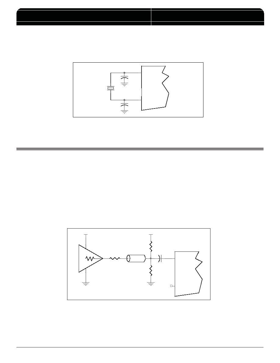
LVCMOS TO XTAL INTERFACE
The XTAL_IN input can accept a single-ended LVCMOS signal
through an AC couple capacitor. A general interface diagram is
shown in
Figure 3. The XTAL_OUT pin can be left floating.
The input edge rate can be as slow as 10ns. For LVCMOS
inputs, it is recommended that the amplitude be reduced from
full swing to half swing in order to prevent signal interference
with the power rail and to reduce noise. This configuration
requires that the output impedance of the driver (Ro) plus the
series resistance (Rs) equals the transmission line impedance.
In addition, matched ter mination at the crystal input will
attenuate the signal in half. This can be done in one of two
ways. First, R1 and R2 in parallel should equal the transmission
line impedance. For most 50
Ω applications, R1 and R2 can be
100
Ω. This can also be accomplished by removing R1 and
making R2 50
Ω.
FIGURE 3. GENERAL DIAGRAM FOR LVCMOS DRIVER TO XTAL INPUT INTERFACE
XTAL_IN
XTAL_OUT
VCC
R2
Ro
R1
Zo = 50
Rs
VCC
.1uf
VDD
Zo = Ro + Rs
CRYSTAL INPUT INTERFACE
The ICS841602I has been characterized with 18pF parallel
resonant crystals. The capacitor values shown in
Figure 2 below
FIGURE 2. CRYSTAL INPUt INTERFACE
were determined using a 25MHz, 18pF parallel resonant crystal
and were chosen to minimize the ppm error.
C1
27p
X1
18pF Parallel Crystal
C2
27p
XTAL_OUT
XTAL_IN
发布紧急采购,3分钟左右您将得到回复。
相关PDF资料
ICS841608AKI
IC CLOCK GENERATOR 32-VFQFPN
ICS841S012DKILF
IC FREQ SYNTHESIZER 56VFQFN
ICS842023BGLF
IC CLK GEN ETHERNET 25MHZ 8TSSOP
ICS8421002AGILF
IC FREQ SYNTHESIZER 20-TSSOP
ICS8422002AGILF
IC SYNTHESIZER LVHSTL 20-TSSOP
ICS8427DY-02LF
IC SYNTHESIZER 500MHZ 32-LQFP
ICS843001AG-123LF
IC SYNTHESIZER LVPECL 8-TSSOP
ICS843001AG-21LFT
IC SYNTHESIZER LVPECL 24-TSSOP
相关代理商/技术参数
ICS841602AGILFT
功能描述:IC CLOCK GENERATOR 28-TSSOP RoHS:是 类别:集成电路 (IC) >> 时钟/计时 - 时钟发生器,PLL,频率合成器 系列:HiPerClockS™, FemtoClock™ 标准包装:1,000 系列:- 类型:时钟/频率合成器,扇出分配 PLL:- 输入:- 输出:- 电路数:- 比率 - 输入:输出:- 差分 - 输入:输出:- 频率 - 最大:- 除法器/乘法器:- 电源电压:- 工作温度:- 安装类型:表面贴装 封装/外壳:56-VFQFN 裸露焊盘 供应商设备封装:56-VFQFP-EP(8x8) 包装:带卷 (TR) 其它名称:844S012AKI-01LFT
ICS841604AGILF
功能描述:IC CLOCK GENERATOR 28-TSSOP RoHS:是 类别:集成电路 (IC) >> 时钟/计时 - 时钟发生器,PLL,频率合成器 系列:HiPerClockS™, FemtoClock™ 标准包装:2,000 系列:- 类型:PLL 频率合成器 PLL:是 输入:晶体 输出:时钟 电路数:1 比率 - 输入:输出:1:1 差分 - 输入:输出:无/无 频率 - 最大:1GHz 除法器/乘法器:是/无 电源电压:4.5 V ~ 5.5 V 工作温度:-20°C ~ 85°C 安装类型:表面贴装 封装/外壳:16-LSSOP(0.175",4.40mm 宽) 供应商设备封装:16-SSOP 包装:带卷 (TR) 其它名称:NJW1504V-TE1-NDNJW1504V-TE1TR
ICS841604AGILFT
功能描述:IC CLOCK GENERATOR 28-TSSOP RoHS:是 类别:集成电路 (IC) >> 时钟/计时 - 时钟发生器,PLL,频率合成器 系列:HiPerClockS™, FemtoClock™ 标准包装:1,000 系列:- 类型:时钟/频率合成器,扇出分配 PLL:- 输入:- 输出:- 电路数:- 比率 - 输入:输出:- 差分 - 输入:输出:- 频率 - 最大:- 除法器/乘法器:- 电源电压:- 工作温度:- 安装类型:表面贴装 封装/外壳:56-VFQFN 裸露焊盘 供应商设备封装:56-VFQFP-EP(8x8) 包装:带卷 (TR) 其它名称:844S012AKI-01LFT
ICS841608AKI
功能描述:IC CLOCK GENERATOR 32-VFQFPN RoHS:否 类别:集成电路 (IC) >> 时钟/计时 - 时钟发生器,PLL,频率合成器 系列:HiPerClockS™, FemtoClock™ 标准包装:1,000 系列:- 类型:时钟/频率合成器,扇出分配 PLL:- 输入:- 输出:- 电路数:- 比率 - 输入:输出:- 差分 - 输入:输出:- 频率 - 最大:- 除法器/乘法器:- 电源电压:- 工作温度:- 安装类型:表面贴装 封装/外壳:56-VFQFN 裸露焊盘 供应商设备封装:56-VFQFP-EP(8x8) 包装:带卷 (TR) 其它名称:844S012AKI-01LFT
ICS841608AKILF
功能描述:IC CLOCK GENERATOR 32VFQFPN RoHS:是 类别:集成电路 (IC) >> 时钟/计时 - 时钟发生器,PLL,频率合成器 系列:HiPerClockS™, FemtoClock™ 标准包装:2,000 系列:- 类型:PLL 频率合成器 PLL:是 输入:晶体 输出:时钟 电路数:1 比率 - 输入:输出:1:1 差分 - 输入:输出:无/无 频率 - 最大:1GHz 除法器/乘法器:是/无 电源电压:4.5 V ~ 5.5 V 工作温度:-20°C ~ 85°C 安装类型:表面贴装 封装/外壳:16-LSSOP(0.175",4.40mm 宽) 供应商设备封装:16-SSOP 包装:带卷 (TR) 其它名称:NJW1504V-TE1-NDNJW1504V-TE1TR
ICS841608AKILFT
功能描述:IC CLOCK GENERATOR 32-VFQFPN RoHS:是 类别:集成电路 (IC) >> 时钟/计时 - 时钟发生器,PLL,频率合成器 系列:HiPerClockS™, FemtoClock™ 标准包装:1,000 系列:- 类型:时钟/频率合成器,扇出分配 PLL:- 输入:- 输出:- 电路数:- 比率 - 输入:输出:- 差分 - 输入:输出:- 频率 - 最大:- 除法器/乘法器:- 电源电压:- 工作温度:- 安装类型:表面贴装 封装/外壳:56-VFQFN 裸露焊盘 供应商设备封装:56-VFQFP-EP(8x8) 包装:带卷 (TR) 其它名称:844S012AKI-01LFT
ICS841608AKIT
功能描述:IC CLOCK GENERATOR 32-VFQFPN RoHS:否 类别:集成电路 (IC) >> 时钟/计时 - 时钟发生器,PLL,频率合成器 系列:HiPerClockS™, FemtoClock™ 标准包装:1,000 系列:- 类型:时钟/频率合成器,扇出分配 PLL:- 输入:- 输出:- 电路数:- 比率 - 输入:输出:- 差分 - 输入:输出:- 频率 - 最大:- 除法器/乘法器:- 电源电压:- 工作温度:- 安装类型:表面贴装 封装/外壳:56-VFQFN 裸露焊盘 供应商设备封装:56-VFQFP-EP(8x8) 包装:带卷 (TR) 其它名称:844S012AKI-01LFT
ICS841608I
制造商:IDT 制造商全称:Integrated Device Technology 功能描述:FEMTOCLOCKS CRYSTAL-TO-HCSL CLOCK GENERATOR VCO: 500MHz